Projects
Manufacturing Engineering Internship @ Mercury Systems
Portfolio
Interning @ Mercury System's Microelectronics Packaging Center in Phoenix
Over the span of almost two years, I worked at Mercury Systems as a manufacturing engineering intern. This was at the Phoenix site, which operates on all fronts regarding printed circuit board fabrication and packaging. This was a continuous experience in that, regardless of the semester I found myself enrolled in, I was employed and actively working. The time that I spent here was split across various functions. My core responsibilities involved supporting manufacturing operations for our microelectronics production floor, but it also included some work in a wafer packaging cleanroom and a failure analysis lab.
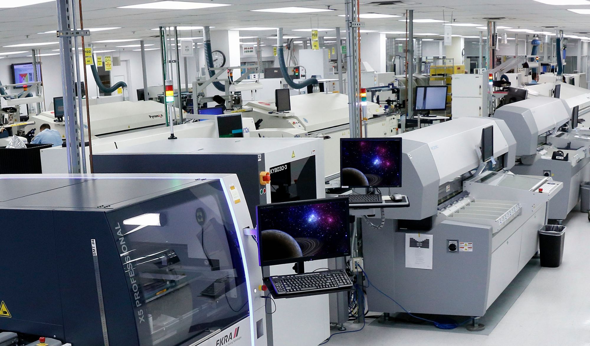
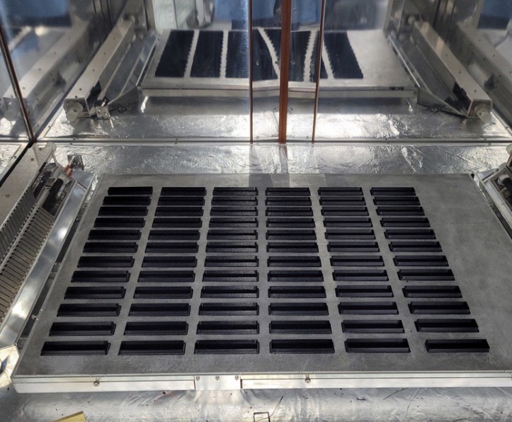
Picture: General Printed Circuit Board Fabrication & Packaging Floor, 1st View
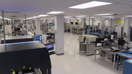
Picture: General Printed Circuit Board Fabrication & Packaging Floor, 2nd View
Responsibilities as a Manufacturing Engineering Intern
I worked in a team of about 15 engineers during this time. While my team was split into product and manufacturing engineers, since I was the sole intern of the group, I had the pleasure of being exposed to many things. I got to learn a little bit about mechanical design, manufacturing operations, electrical systems, and more.
Picture: AM Design Software Workflow | Siemens NX (1st), nTop (2nd), Simufact Additive (3rd), Materialise Magics (4th), GOM Inspect (5th)
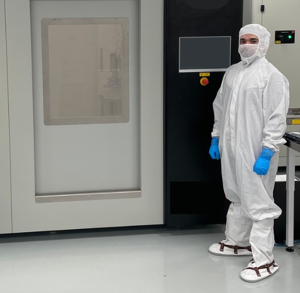
For example, some of the projects I was involved in were to support our cleanroom floor that was dedicated to wafer packaging. The goal was to bring about new business in the form of building end-to-end packaging processes for 200mm [8"] and 300mm [12"] wafers from the ground up. So to be an effective aide to the engineers, I learned how to use all the equipment in our wafer cleanroom. This included dicing saws, plasma clean stations, dispensing equipment, metrology equipment, etc.
It's important to note that the software workflow is broadly linear, but this isn't always the case. Sometimes (as you'll see below), nTop, which can generate complex TPMS structures may not actually be needed for a given part. As such we may skip or return to certain applications as needed. Ultimately, however, this is the general process in bringing a part from idea in NX to reality in GOM Inspect (the step where we scan the metal 3D print)!
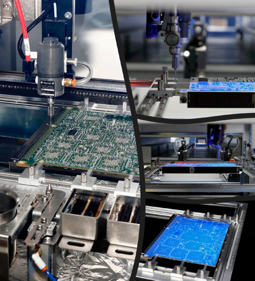
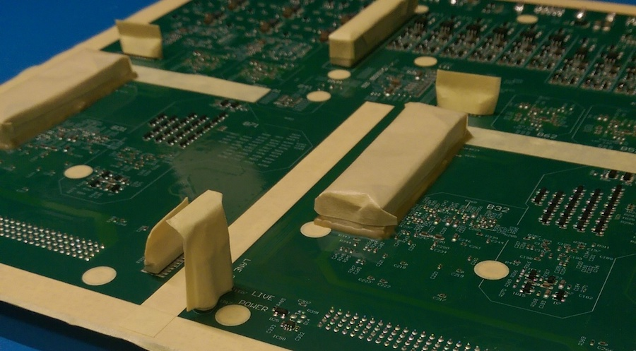
Picture: PCB Manufacturing Process | Conformal Coating (Left), Conformal Coating Inspection (Right, all three)
Picture: Coupon Board Inspection under High-powered Microscope
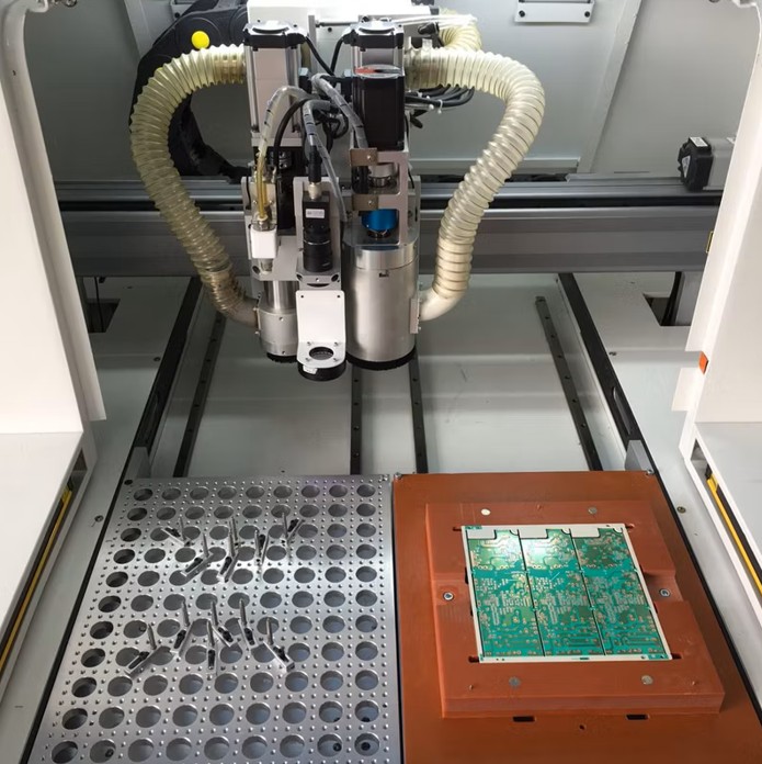
Picture: PCB Router Setup for Depaneling
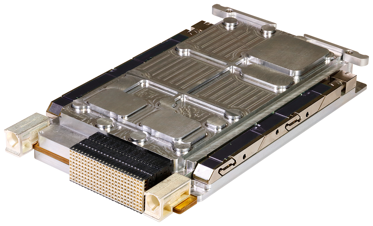
Picture: Mercury Systems Rad-Tolerant SSDR, Fully Assembled
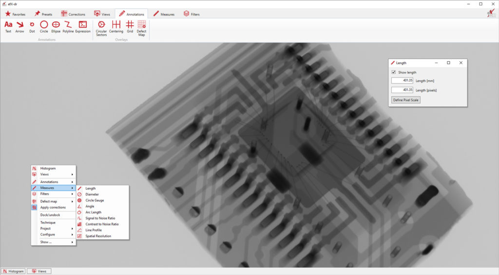
Picture: 3D CT X-ray Scan of PCB
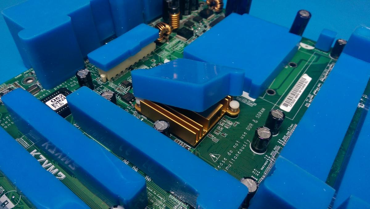
Picture: Conformal Coating Masking Boot Prints via Essentium Industrial Printer
Picture: Teledyne LeCroy WavePulser 40iX's Time Domain Reflectometry Software
Picture: GOM Inspect (now ZEISS Inspect) User Interface
Picture: Teledyne LeCroy WavePulser 40iX's Time Domain Reflectometry Software
Picture: Teledyne LeCroy WavePulser 40iX's Time Domain Reflectometry Software
Mechanical Subsystem Design
H
Recovery, Redundancy, and Contingency Plans
f
Manufacturing and Procurement
I
Verification
I validated designs through CMM inspections, FEA for structural loads, and thermal cycling tests, achieving TRL 7 for mechanical subsystems.
Summary
- Delivered mission-ready designs for a 2030 lunar launch under $300M budget.
- Achieved TRL 7, enabling lunar pit exploration.
- Mastered CAD, FEA, and systems integration.
- Led a top-performing team, enhancing my aerospace expertise.